

Stan Voynick has returned for the “Ask an Expert” web series where we talk about our thermal cameras and the technology behind them. Today, he is going to be talking about microbolometers, which are the sensors at the heart of our long-wave imaging systems.
A scientific instrument that measures incoming radiation
A bolometer is a scientific instrument that measures incoming radiation and light by changing temperature. A bolometer could be a centimeter or more in size. If you took a bolometer outside and put it in sunlight, you could measure how intense the rays are from the sun, how much light, how much heat, how much energy is falling from sunlight.
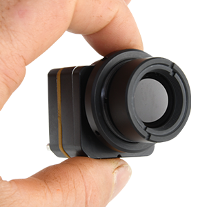
If we take the bolometer instrument, which could be a centimeter in size, shrink it down to ten microns, and then build an array of hundreds or thousands of those bolometers next to each other, it becomes a microbolometer array, because we’ve shrunk them down. The sensor inside the Tenum 640 is a microbolometer array. When we put a lens on the front of that sensor and we focus an incoming scene on that array of bolometers, each one of those microbolometers now can detect how much light is falling at that spot in the scene. We bring those signals out and turn them into an infrared image.
You must create bolometers out of a material that is suitable to the task. The material has to be able to absorb the correct wavelengths of light that you’re interested in efficiently. It has to have electrical resistance characteristics that work in order to be able to remeasure its resistance, which relates to its temperature change. Amorphous silicon and vanadium oxide are the two most commonly used materials for building these instruments. In our case, most of the microbolometers that we work with are made out of vanadium oxide as the technology has better stability in the image and can be compacted into smaller arrays for low-swap applications.
The process for building arrays at the microbolometer level is actually not unlike the process for making microchips that we use in our cell phones and our computers. You start with wafers of material. Certain materials are deposited onto the wafer. Then patterns are etched. Other materials can be deposited upon that. The original materials can be etched away in the end for microbolometer fabrication. You end up with structures that on the ten micron scale rise up off of the substrate and have little plateaus on top, which are the receiving elements for the incoming light.
When light falls on a bolometer is is measuring temperature change by measuring its resistance in the material the sensor is made from. When you shrink it down to a microbolometer and make an array of them you can plug in a device called a readout integrated circuit. Some people call it an ROIC or even pronounce that as a ROIC and that’s an electronic circuit that sits right next to that detector array and sequentially and very quickly measures the resistance of each of those hundreds of thousands of microbolometers to read out. This process of reading out the resistance from the sensor signal then becomes the electronic representation of the image, which can then be transferred out over various kinds of interfaces like gigabit Ethernet, USB or direct CMOs, parallel output, and then received by a computer or a display for processing and viewing.
We talked about there being thousands, tens of thousands of microbolometers in these sensor arrays, we can be more precise. A Tenum 640, which has a 640 x 512 image format, contains roughly 320-327,000 microbolometers in its array. Going up a level to the Tenum 1280, which is a 1280 HD camera, has about 1.3 million little 10micron microbolometers. At the heart of our Vayu HD and Vayu HD-I cameras is the Athena sensor from BAE systems. This sensor is 1920 pixels wide by 1200 pixels high and contains about 2.5 million microbolometers in its array.
Why the difference over such a wide range?
There are different applications for infrared imaging. There may be applications where size is most important, and with a small array you can have smaller optics. If that meets your particular imaging needs, that’s a fine lower cost way of accomplishing your goals. On the other hand, there may be applications where you may want a much wider field of view and will need a larger optic. In this case, something like an Athena 1920 x 1200 sensor would give you very wide field of view and good resolution all at the same time.
I’ve talked about how small microbolometer images are individually, and I’ve talked about how many elements there are in an array, but let’s talk about what that means in terms of the size of the image that we’re focusing on. On the front of the Athena is a piece of glass covering the microbolometer array, but it’s actually a more exotic material than that. This piece of glass is where the light comes through and strikes the sensor which is enclosed behind it. The Athena has 12 micron pixels, in other words, each pixel is 12 micron square. If you line up 1,920 of those pixels horizontally, that ends up being about a 2.4 centimeters wide. 1,200 microns vertically is almost an inch, or 1.4 centimeters. This give you an array that’s 2.4 centimeters by 1.4 centimeters in size, which is the approximate size of the glass cover. It’s that large number of pixels that gives the Athena and our Vayu HD and HD-I cameras their resolution with their ability to have a really wide field of view at the same time as maintaining HD resolution.
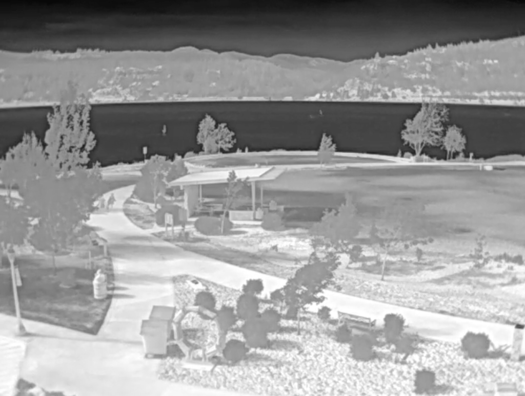
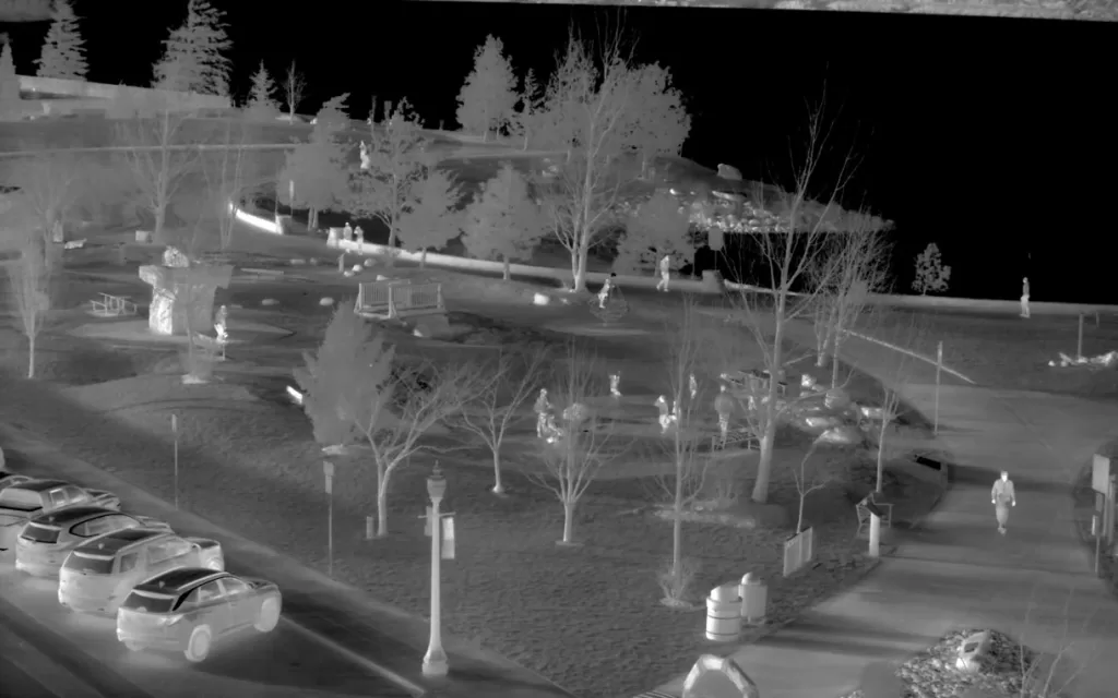
Imagery from our Vayu HD with Athena Sensor


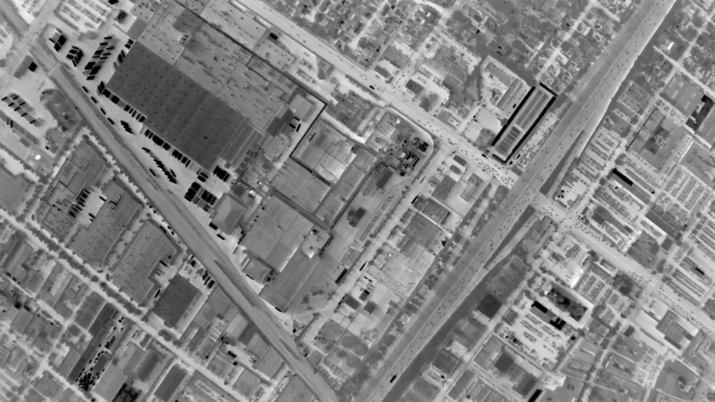

We call it situational awareness, where you can see the big picture all at once, but you’re not giving up resolution at the fine detail range. You can have that big picture situational awareness, but still pick out small details of interest in the scene. You need a large number of pixels to do that.
You ruin a good microbolometer array with a mediocre lens
You’ve got to put good optics, or a good lens in front of an HD sensor in order to get all those pixels to work together. Deliver a good quality image to that focal plane or array of microbolometers to get the big picture and the detail at the same time.
Thanks for reading this edition of our Ask an Expert series where we discussed microbolometers. I hope you found it informative and interesting. I encourage you to keep learning about IR technology through the videos and the other parts of our website. If you have questions or comments, please send us a message on the form below. Thanks for reading!